Printed circuit board, pcb, milling

Home Model Engine Machinist Forum

Help Support Home Model Engine Machinist Forum:

This site may earn a commission from merchant affiliate links, including eBay, Amazon, and others.
Troutsqueezer said:
I am the Responsible Engineer for a number of projects in a well-known company. For our "PCB's" we are currently down to trace widths of 9um (0.000354330 inches, 0.354330708 mils). Via drill size is down to 67um (0.002637795 inches).
Repeatability is good at around 300 million units @ >99% yield. ;D

Oh, man.
 
@ troutsqueezer

Very impressive track widths - do you know what process is used to achieve them ? I assume that the copper thickness must be very small to prevent under etching.

Best Regards

picclock
 
ttrikalin said:
Jeremy,
does the router have servos or steppers?

Steppers. It's not all that rigid (built of Acrylic sheets, HDPE blocks, and some EMT conduit), but it does the job. I'm currently in the process of building a much more robust machine to replace it on PCB duty, but for everything else I throw at it, it performs admirably. Here's an example of some work I did with it. http://tinyworkshop.org/projects/making-coasters/
 
picclock said:
@ troutsqueezer

Very impressive track widths - do you know what process is used to achieve them ? I assume that the copper thickness must be very small to prevent under etching.

Best Regards

picclock

I do indeed. It is a buildup process where the copper is added to the prepreg (dielectric material, like FR4 but different), much like you would see with a silicon buildup process using epitaxy. So it is an additive process that uses a mask. These buildup layers are placed on a thicker core layer which is laminated and thick (relatively speaking - 400um) to provide stiffness so that the package does not warp with temperature. The process for core layers is subtractive (etched) so they are much like standard PCB's and as such the traces must be much wider at a minimum of 75um. Power delivery is usually accomplished using these laminated layers and not the buildup layers. So then, the 9um traces on buildup are used for signal IO's and not power delivery.

These are the substrates that silicon is attached to in order to connect to the system/mother boards. They are typically 6 to 18 layers.

Copper thickness is 15um. Since there is no etching, under etch isn't a problem.

More than you wanted to know, right? ;)
 
Hi troutsqueezer

>>More than you wanted to know, right? Wink

Very informative, and it explains how you manage those exceptionally thin widths. Are you able to tell more about how the masking and copper deposition works? This is just to satisfy my curiosity cos basically I'm nosey and like to know everything. ;D

Best Regards

picclock
 
Hi Picclock

I've tried overhead film many many years ago without any luck - the dark areas weren't dark enough after printing on the laser printer .... :(

So I'm very curious - what brand film are you using ?
 
I also use photoresist board (Kinsten brand)
I've never used transparency film, cheap tracing paper(I think it is actually a plastic) from a stationary supply works fine for me, been using it for over a decade without issue.

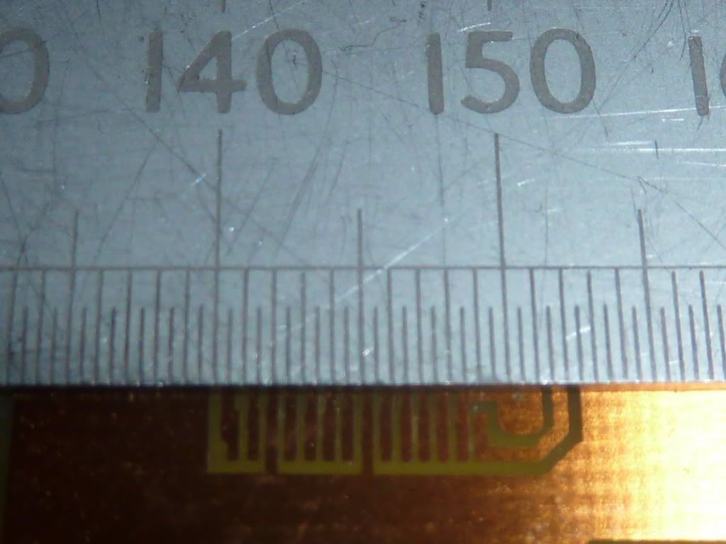
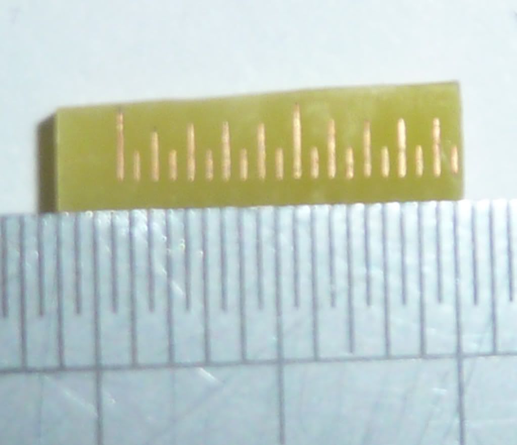
Photoresist has amazing resolution, early-on I was getting pin holes and rough edges on my tracks which drove me insane. Trying to find the problem I eventually used a low powered microscope to compare the tracks and the laser prints, the tracks were exact copies. The rough edges were due to the 600LPI resolution of the printer!
I also was worried about the density of laser prints when I started, but it has never been an issue except for the occasional tiny pin hole which I think is more dependent on the quality of the printer.

The biggest issue I have had is distortion. I have never once used a laser printer that scales correctly.
To correct, I print a test page with an x-y scale I made up in CAD years ago to fit an A4 sheet, then measure the error with a rule and correct for it when I print the artwork. Check again and things are usually pretty close.
It's not a big issue for thru-hole components, but can be for fine-pitch SMD or BGA chips.

I simply use the Sun to expose my boards, it's cheap(free!) and takes about 30 seconds to a min or so depending on season(and latitude). Only problem is it is not always around!

A hang-over from my photography darkroom days, I used to do an exposure test strip; print a strip of numbers in 5 second increments and then expose a thin slice of board, uncovering a new number every 5 seconds from the 60(or whatever) second end to the 5 second end. Develop, strip, etch and check for best exposure.
If that doesn't make any sense, do a google search for "darkroom test strip" ;)
I've found the Kinsten brand resist has a fair exposure latitude anyway. Possibly the same for other brands.

I had something else to share too, but forgot what it was, I have blah blah blah long enough now anyway! haha
 
A lot of this sounds familiar. Make a film positive. sandwich the positive to a photosensitive material expose to a UV light source. Develop and wash.. I leaned in the days of dark rooms and film both for cameras and printing trades (Big Process cameras) As tedious cumbersome and chemical intensive as the old (1980s) processes were the image density was fantastic. In the mid 80 i worked in a new Art dept for a company that printed Microscope slides Cell Line (now owned by Fischer) we used a Photo mechanical transfer system) more convenient but harder to control the density. I have also made silk screens at home and worked with laser generated film positives Again tough to get good density. A good tip on test strips I have done a few in my time.
Maybe one I will venture to make a few pcbs but so many hobbies so little time.
But kicking back to the old ways the simplest way I know to make a film positive is ruby lith just cut with an exacto knife and peel away
http://www.ulano.com/knifecut/masking.htm
India ink on velum is another old stand by but have not actually used it.
Tin
 
@Admiral_dk

I just use OHP projector film, normally sourced from Staples - cheapest I can get.

Seems any laser printer will work (I've tried 3). Just print two copies one after the other, then tape the two together accurately so that everything lines up perfectly. Place mask on glass then board on mask and weight down with a book or two. You must use a lamp of the correct wavelength for the resist. If in doubt do a test piece by moving a piece of card under the mask as the exposure takes place, say 1 or 2 cms every minute. When you develop it you will have the optimum exposure time. Random picture I just took.

P1000569.jpg


Shows an old board for a stepper motor controller. The tracks there are around 12 thou, although I have done much smaller. I seem to have lost a lot of my original photos when I upgraded my PC.

Hope this helps

Best Regards

picclock

PCB.jpg


picture of 5 thou tracks done for scaling errors originally.
 
Thanks Picclock

The quality must be a lot better than when I tried this many years ago, but that's the way of the computer world (and others). Back then you could look through the black print on the film - I haven't got a clue if it's mostly the printers, toner or the film that has improved (or a combination). I'll try to get some film at work to try out.

Thanks for the info about the handling of the film too - though I knew that, there might be others here that can use it.

I've made some very fine pitched PCB traces in my time, but that has always been photolabs or a Gerber-plotter making the films for those to bee good enough for production and prototypes - no good using your debug time on the design only to discover that the proto PCB has errors from a bad film or etch. This is something I can live with on hobby projects, but not in a professionally time pressed R&D project. Now I almost exclusively design Pro Audio for musician, so it's big traces in order to survive the harsh environment.
 
picclock said:
Hi troutsqueezer

>>More than you wanted to know, right? Wink

Very informative, and it explains how you manage those exceptionally thin widths. Are you able to tell more about how the masking and copper deposition works? This is just to satisfy my curiosity cos basically I'm nosey and like to know everything. ;D

Best Regards

picclock

Greetings picclock,

There is a lot to it, much more than I could begin to type. Here is a link to a document that touches on the various aspects of the technologies involved. The document is about 10 years old I think and the technology is constantly moving forward but it gives a pretty good overview of the processes. Skip to page 16 and it begins talking about buildup.

This technology is relative to BGA and PGA type substrates (Ball Grid Array and Pin Grid Array - fancy names for how the designs attach to the mother boards).


http://smithsonianchips.si.edu/ice/cd/PKG_BK/CHAPT_11.PDF
 
Hi Troutsqueezer

That was definitely more than I wanted to know. But very interesting.

In a former life I worked on automated PCB testing equipment, run by a quaint PDP8 (if your old enough to remember). I think it was the first in the world. I was mainly involved in the design of some peripherals which allowed testing of the onboard components. I remember it used hundreds of reed relays and would test blank or loaded pcb's. A blank board test for breaks or shorts would take about a tenth of a second. The nice thing was that once a 'bed of nails' jig was made for the board, each 'nail' corresponding to a track end or test node, a blank known good board could be loaded and the program would store the relative connection points. After that all other boards tested to the same spec.

Many thanks for the info

Best Regards

picclock
 
picclock said:
In a former life I worked on automated PCB testing equipment, run by a quaint PDP8 (if your old enough to remember). .............The nice thing was that once a 'bed of nails' jig was made for the board, each 'nail' corresponding to a track end or test node,

That takes me back, remind me what it was called? Its buried somewhere in the fug that was a brain but I can't dig it out. I recall it was the bees knees in ATE at the time

On laser film I use is "laserstar" its for making PCB masks, its opaque. I did use OHP slides for a while but it wasn't that good as it bled a bit and the track definition wasn't that good.

http://www.megauk.com/artwork_films.php

Pete
 
Anybody here go back to using rubylith film and black tape on acetate over a light window to do their designs? I still see black spots to this day. :)
 
I used tape and donuts when I was a kid. And the letraset style rub-off I.C. pad patterns.
Might still have some floating around in a box somewhere.

Rubylith, if it is what I think it is, was something I used to see my Oldman hunched over for hours on end.
When I was a kid he owned a screen printing business.
Squeegee in hand by day, Rotring scalpel in hand cutting the stencils by night.
He also had a huge(HUGE!) process camera. He used to get people from all over the place hiring time on it.
He tells me this included some silicon-fab designers(IC's). Late 70's early 80's so my memories are hazy.
 
Of course it is not relevant. However, you have shared great information. Thanks for sharing.

--------------------
 
Last edited by a moderator:
This is a very interesting new idea but unfortunately I don’t use Eagle. Can I use OrCAD/ARES/ADS with this? Can you guess if I’d face any isses? Also, you mentioned that you wrote a python code but the rotation or offsets could have been set from the Eagle, is there any advantage of doing this using a code instead of built in functions from the CAD software? Sorry for so many questions.
 
Back
Top